

Validation of On-Wafer VNA Systems
©2006 IEEE 68th ARFTG, December 2006
Validation ofOn-Wafer Vector Network Analyzer Systems
J. Randy Fenton
Cascade Microtech, Inc., Beaverton, 2430 NW 206th Avenue, Beaverton, OR, 97006, USA
Abstract — The case study described in this paper applies a known vector network analyzer comparison technique to an on- wafer measurement environment. The purpose is to investigate and expand upon this technique’s applicability for use in validating an on-wafer VNA system of unknown accuracy by comparing it to an on-wafer VNA system of trusted accuracy. The technique involves taking calibrated S-Parameter measurements with each system over a set of validation devices and calculating the measurement differences between the two systems. These differences are then compared to the estimated repeatability uncertainty bounds of the two VNAs in order to validate or invalidate the unknown system’s capabilities. Results and limitations of this procedure are discussed.
Index Terms — Calibration, On-Wafer, Vector Network Analyzer, VNA, Validation
I. INTRODUCTION
Throughout the electronics industry, users of on-wafer vector network analyzer (VNA) measurement systems seek to answer one simple question on a daily basis: Once I have calibrated my on-wafer VNA system, how can I have confidence that it is able to make accurate on-wafer S- Parameter measurements?
To help answer this question, a variety of calibration comparison studies have been published over the last fifteen years [1]-[4]. These studies quantify measurement differences that result from the use of different on-wafer and/or off-wafer calibration standards and techniques (such as SOLT, LRRM, LRM and TRL). Many ofthese studies employ the calibration comparison techniques shown in [1] and [2] developed at the National Institute of Standards and Technology (NIST). The reports compare various on-wafer calibration techniques to each other and to the well-defined NIST Multi-line TRL calibration method [5]. As a result, there is a good understanding throughout the industry regarding the strengths and weaknesses of the most commonly used on-wafer calibration techniques.
Given this understanding, a user is able to choose a calibration technique that best meets his or her requirements. However, once this calibration has been performed, there exists a need to validate the calibrated VNA system before measurements are made.
While the calibration comparison techniques in [1] and [2] are extremely powerful, they are not practical as daily on- wafer measurement system validation checks (and indeed, were never intended to be).
However, the method of comparing VNA measurement systems described in [6] is worth investigating as an on-wafer VNA validation tool. This technique involves taking calibrated S-Parameter measurements using two distinct VNA systems over a specific set of validation devices and calculating the differences in data between the two systems. These differences are then compared to the estimated repeatability uncertainty of the VNAs in order to determine if the two VNAs agree. If the VNAs do not agree within the repeatability limits it can be concluded that residual errors unaccounted for by calibration within the systems exceed the repeatability errors.
Thus, this technique can be used to determine whether or not one VNA is able to reproduce specific measurement results from another VNA within an agreed limit. Taken a step further, this technique can be used to compare an on- wafer VNA measurement system of unknown accuracy to an on-wafer VNA measurement system of trusted accuracy in order to validate the unknown system’s measurement capability.
This paper will present a case study ofthis nature.
It is important to note that this comparison technique is only valid for the specific set of validation devices used during the experiment. That is, it does not guarantee accurate measurements of other devices of different materials and/or geometries existing on different substrates. However, for many users this quick and convenient validation check provides enough important feedback to either gain or lose confidence in their measurement system.
II. PURPOSE
The purpose of this case study is investigate and expand upon the vector network analyzer comparison technique described in [6] for use in validating an on-wafer VNA measurement system of unknown accuracy by comparing it to an on-wafer VNA measurement system of trusted accuracy.
The study will compare two distinct on-wafer VNA measurement systems. One system will be designated the Reference system and the other the Test system. Data that represents the overall results of the study will be presented.
Another purpose is to outline a detailed on-wafer VNA validation procedure that can be employed by other users in the on-wafer measurement community.
|
Offset 25Ω Resistor Long Offset 25Ω Resistor Offset 100Ω Resistor Offset 150Ω Resistor Offset 300 Ω Resistor Offset Short |
|
Capacitor |
The study will also lend insight into what types of on-wafer structures are recommended for this type of experiment and will provide guidelines for the analysis.
IV. MEASUREMENT SYSTEMS AND STRUCTURES
A. Reference and Test System Details
This case study compared two distinct on-wafer VNA measurement systems – a Reference system and a Test system.
The Reference System consisted of:
Cascade Microtech S300 probe station, Agilent E8361A PNA, 50GHz Gore RF test cables, Cascade Microtech 50GHz Infinity GSG 150µm opposing probes, Cascade Microtech 101-190 impedance standard substrate, WinCal XE calibration and measurement software [7].
The Test System consisted of:
Cascade Microtech 12K probe station, Agilent E8364A PNA, 50GHz Gore RF test cables, Cascade Microtech 50GHz Infinity GSG 150µm opposing probes, Cascade Microtech 101-190 impedance standard substrate, WinCal XE calibration and measurement software [7].
Each network analyzer was set identically in terms of frequency range, number of points, power level, IF bandwidth and averaging. The frequency range was 0.25 – 50GHz. In addition, the LRRM calibration technique was used for each set ofmeasurements.
B. Validation Structures
A variety of passive on-wafer validation structures were studied and carefully chosen for this case study. Some structures were chosen for their reflective properties representing different areas of the Smith chart while others were chosen for their transmission properties having varying degrees of loss.
The majority of the on-wafer validation structures chosen for this case are found on the Cascade Microtech General Purpose (PN 005-016) and the LRM (PN 101-190) impedance standard substrates. However, some of the structures are experimental only.
The validation structures include:
40ps Transmission Line
40ps Open Stub
10dB Attenuator
20dB Attenuator
12.5Ω Resistor
25Ω Resistor
50Ω Resistor
Inductor
Fig. 1 shows the S11 Smith chart data for the family of validation devices used in this study.
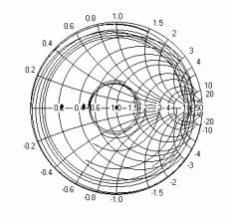
Fig. 1 S11 Smith chart data for family ofvalidation structures
III. COMPARISON PROCEDURE
The on-wafer VNA comparison procedure used in this study is described below. Cascade Microtech’s WinCal XE calibration and measurement software [7] with its new Calibration Validation Application Tool Kit was used to automate all probe station movement, all calibrations and calibration comparisons, all measurements and data manipulation, and all report generation.
Step 1: Perform an on-wafer calibration on the Reference
system and save as RefCal1.
Step 2: Measure all Validation Structure(s) sequentially on
the Reference system using RefCal1. Save all data.
Step 3: Immediately after Step 2, perform a second on-wafer
calibration on the Reference system and save as
RefCal2.
Step 4: Perform an on-wafer calibration on the Test system
and save as TestCal1.
Step 6: Measure all Validation Structure(s) sequentially on
the Test system using TestCal1. Save all data.
Step 7: Immediately after Step 6, perform a second on-wafer
calibration on the Test system and save as TestCal2.
Step 8: Calculate the Error Vector Magnitude (EVM) for
each validation structure measured on the Reference system and the Test system.
EVMij = |SAij – SBij| where SAij is the validation structure S-Parameter data taken from the Reference system and SBij is the validation structure S- Parameter data taken from the Test system.
A family of validation structures will result in a family of EVMs consisting of EVMV1ij, EVMV2ij,
©2006 IEEE 68th ARFTG, December 2006
EVMV3ij etc. where superscripts V1, V2, V3, etc. denote the different validation structures measured.
Step 9: Extract the resulting error terms from RefCal1 and
RefCal2 and use the NIST Calibration Comparison technique [2] to determine the Reference system’s repeatability limits (∆AR).
Step 10: Extract the resulting error terms from TestCal1 and TestCal2 and use the NIST Calibration Comparison technique [2] to determine the Test system’s repeatability limits (∆BR).
Step 11: Add the Reference system’s repeatability limits to the Test system’s repeatability limits to obtain the overall repeatability bounds for the comparison (∆AR+∆BR).
Step 12: Plot EVMV1ij, EVMV2ij, EVMV3ij, etc. vs. (∆AR+∆BR) to see if the Reference system and Test system agree to within the repeatability limits for each validation structure.
Step 13: Plot each validation structure Reference system S- Parameter measurement data SAij ± ∆AR to show Reference data with Reference system repeatability bounds.
Step 14: Determine the maximum EVMij from the family of EVMs at each frequency and store this as max(EVMij).
Step 15: Plot max(EVMij)) vs. (∆AR+∆BR) to show worst case.
IV. COMPARISON RESULTS
This study used the calibration comparison technique described in [2] applied to two identical calibrations from the same system to estimate that system’s repeatability bounds. One calibration was performed immediately before the validation structure measurements and the second calibration was performed immediately after. This way the calibration comparison also estimates the system’s drift during the time taken to make the measurements.
WinCal XE [7] was used to calculate the repeatability bounds two different ways.
The first method performed the calibration comparison while applying the error terms to the S-Parameter measurement data for each particular device. This yields a repeatability bound applicable specifically to that device. Using this method, each device has its own unique repeatability bound for each system.
The second method calculated the worst case repeatability bounds for each system by applying the error terms to an S- Parameter data set that consisted of all terms set equal to one.
Following the above procedure, the error vector magnitude difference (EVM) between the Reference measurements and the Test measurements for each structure were first calculated.
Repeatability bounds for each system were then calculated for each device using the device-dependant method described above. Each EVM was then compared to the sum of the systems’ applicable repeatability bounds to determine if the systems agreed for each device measurement.
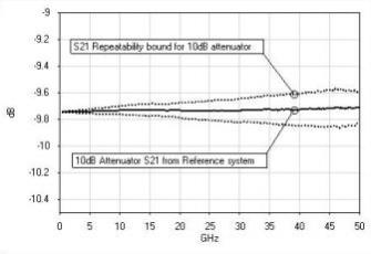
Figures 2 and 3 show the results of S11 and S21 measurements made on the 10dB attenuator. The figure shows the EVM between the two systems plotted against the sum of the repeatability bounds calculated using the 10dB attenuator’s S-Parameter files. This data represents a typical result from this case study where the two systems agreed well within the device-dependent repeatability limits for the measurement of a particular device.
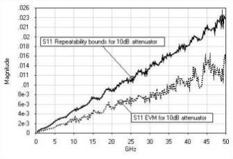
Fig. 2 10dB attenuator S11 EVM vs. 10dB attenuator device-
dependent sum of repeatability bounds
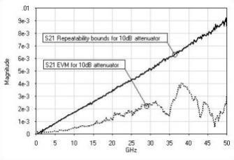
Fig. 3 10dB attenuator S21 EVM vs. 10dB attenuator device- dependent sum of repeatability bounds
Fig. 4 shows the results of S11 measurements made on the inductor. The figure shows the EVM between the two
systems plotted against the sum of the repeatability bounds calculated using the inductor’s S-Parameter files. Note that the repeatability bounds are much larger for the inductor than for 10dB attenuator. This is to be expected as the inductor is
©2006 IEEE 68th ARFTG, December 2006
much more reflective. Also note that the inductor’s EVM approaches the repeatability bounds at high frequencies. This is not surprising as network analyzer residual errors are much more sensitive to the measurement of highly reflective
devices.
Fig. 4 Inductor S11 EVM vs. inductor device-dependent sum of repeatability bounds
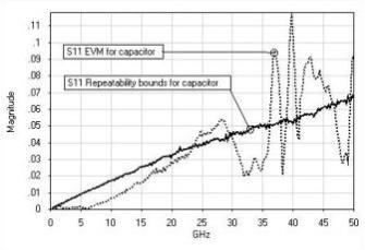
Fig. 5 shows the results of S11 measurements made on the capacitor. The figure shows the EVM between the two systems plotted against the sum of the repeatability bounds calculated using the capacitor’s S-Parameter files. Note that the EVM greatly exceeds the repeatability bounds. Inspection of the capacitor after measurement showed that the capacitor’s probe pads were excessively dirty and somewhat damaged at the time of the Test system measurement. This led to poor probe-to-pad contact resulting in poor measurement results. This illustrates how this validation technique can be used to discover and resolve measurement system problems.
|
of repeatability bounds |
The next part of the analysis consisted of calculating the maximum EVM for each S-Parameter at each frequency point
from the family of device EVMs. This maximum EVMij represents the maximum difference between the two systems
for the set of validation devices. The worst case repeatability bounds for each system were calculated using the worst case method described above. The maximum EVM was then compared to the sum of the worst case repeatability bounds (∆AR+∆BR) to show a worst case scenario. Note that the capacitor EVM data was excluded from the maximum EVMij calculations.
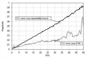
Figure 6 and 7 show the S11 and S21 results of this analysis. In Fig. 6, the maximum S11 EVM falls well below the sum of the worst case repeatability bounds except for at high frequencies where the inductor results described above define the maximum EVM. The maximum S21 EVM of Fig. 7 also falls well below the sum of the worst case repeatability bounds. It is interesting to note that the peak of S21 EVM at higher frequencies is due to the offset 100Ω resistor validation structure data. Given the magnitude of the worst case repeatability bounds, these figures suggest that using the worst case repeatability bounds as the upper limit for pass/fail criteria is a more conservative approach versus using the device-dependant repeatability bounds.
|
repeatability bounds |
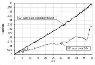
Fig. 7 Maximum S21 EVM vs. worst case sum of S21 repeatability bounds
|
[1] D. F. Williams, R. B. Marks, and A. Davidson, "Comparison of |
©2006 IEEE 68th ARFTG, December 2006
Lastly, the S-Parameter data taken on the Reference system
plus and minus the magnitude of the Reference system uncertainty bounds (SAij ± |∆R|) was plotted for each validation structure. This was found to be a useful graphical
representation of the Reference data during this analysis. Figure 8 shows an example ofthis for the 10dB attenuator.
|
device-dependent repeatability bounds |
V. CONCLUSION
This case study compared two distinct on-wafer network analyzer measurement systems by measuring a family of validation structures and comparing the results.
The results suggest that the Test system was able to reproduce measurements made on the Reference system to within the estimated repeatability bounds of the two systems. The conclusion is that Test system can therefore be trusted for measurements of this family of devices.
As expected, validation devices exhibiting higher reflectivity resulted in higher device-dependent repeatability bounds and larger measurement differences between the two systems. Because network analyzer residual errors are device dependent, it is best to choose a family of validation devices that cover different regions of the Smith chart and that have varying degrees of attenuation.
The estimate of the worst case repeatability bounds was shown to be a more conservative pass/fail criterion for the
Test system than the device-dependent repeatability bounds for each device.
The analysis also uncovered a problem while measuring the capacitor where poor probe contact resulted in poor measurement results.
By automating the entire comparison process using WinCal XE, the technique proved to be a quick and insightful procedure to gain confidence in an on-wafer measurement system ofunknown accuracy.
This useful system comparison technique can also be used to compare and validate on-wafer measurement systems that employ different calibration techniques. This will be the work of future studies.
ACKNOWLEDGEMENTS
The author wishes to thank Dr. Leonard Hayden and the WinCal XE development team consisting of Herje Wikegard, Brian Smith, Nathan Wiegman and Bob New for their assistance and support.
REFERENCES
On-Wafer Calibrations," 38th ARFTG Conference Digest, pp. 68-81, Dec. 1991.
|
comparison method for vector network analyzers," 48th ARFTG Conference Digest, pp. 38-45, Clearwater, FL, Dec. 1996. |
|
probe-tip calibrations," 42nd ARFTG Conference Digest, pp. 37-44, Dec. 1993. |
|
comparison in on-wafer measurement," URSI-GA 2002, Aug. 17-24, 2002. |
|
calibration,” IEEE Trans. Microwave Theory Tech., Vol. 39, pp. 1205-1215, (1991). |
|
comparing vector network analyzers," 50th ARFTG Conference Digest, pp. 107-114, Portland, OR, Dec. 1997. |
[7] WinCal XE, Cascade Microtech, Inc., Beaverton, OR. (Available Fall 2006)
![]()
![]()
![]()
Cascade Microtech, Inc.
2430 NW 206th Ave., Beaverton, Oregon 97006, USA
Toll Free: +1-800-550-3279 Phone: +1-503-601-1000
Europe: +44-1295-812828 China: +86-21-6340-4183
Japan: +81-3-5478-6100 Singapore: +65-6873-7482
Taiwan: +886-3-5722810
Email: sales@cmicro.com http://www.cascademicrotech.com
Copyright © 2006 Cascade Microtech, Inc. All rights reserved.
All trademarks are the property oftheir respective owners.
AR140
Data subject to change without notice