

Test Setup Optimization and Automation for Accurate Silicon Photonics Wafer Acceptance Production Tests
2020 INTERNATIONAL CONFERENCE ON MICROELECTRONIC TEST STRUCTURES, April 6-9, EDINBURGH, UNITED KINGDOM
9.4
Test Setup Optimization and Automation for Accurate Silicon Photonics Wafer Acceptance
Production Tests
Choon Beng Sia1, Tiong Leh Yap2, Ashesh Sasidharan2, Jun Hao Tan2, Robin Chen2, Jacobus Leo2, Soon Leng Tan2 and Guo Chang Man2
1FormFactor Singapore Pte. Ltd.
30 Marsiling Industrial Estate Rd 8, #05-02, Singapore 739193
Telephone: +65 6309 3450, Email: choonbeng.sia@formfactor.com
2GLOBALFOUNDRIES Singapore
60 Woodlands Industrial, Park D Street 2, Singapore 738406
Telephone: +65 6362 2838,Email: guochang.man@globalfoundries.com
Abstract — Implementing energy-efficient optical transceiver modules with silicon photonics (SiPh) and 3DIC technologies will help alleviate the increasing energy consumption for hyperscale data centers. To facilitate effective 3DIC heterogenous integration of these photonics integrated circuits for optical transceivers, high precision, repeatable and reliable SiPh wafer acceptance tests are essential and vital. This paper successfully demonstrated incident angle optimization for optical wafer tests as well as evaluation of a fully automatic SiPh wafer test architecture that is accurate and dependable, achieving excellent test correlations between passive and active devices designed with grating-couplers and edge- couplers.
I. INTRODUCTION
Worldwide data centers and networks for communications currently consume about 8% of the earth’s total energy produced. To meet the increasing demands for cloud storage, computing and various emerging applications such as artificial intelligence, genomics revolution and video transcoding etc., hyperscale data centers are being built around the world at an accelerated pace, with analyst predicting up to 20% of earth's
|
|
total power output consumed in 2030, as shown in Fig. 1 [1]. Optical fiber communications within data centers and the use of Silicon Photonics (SiPh) to implement these optical transceivers present a very attractive option, drastically reducing power consumption, cost and size ofthese transceiver modules.
In addition, the mature silicon CMOS processing technologies and advanced 3DIC packaging technologies both offer an established high-yield production solution to fabricate such silicon-based optical transceivers. For effective heterogeneous integration and packaging of these silicon-based optical transceivers, individual functional chips, for example, logic, photonics and laser must all be tested prior to stacking and packaging. Key wafer test challenges such as optimizing the test setup, correlating results of wafer-level and final product tests, layout rules, test pads standardization and test automations to satisfy high throughput production test requirements, will all be discussed in this paper.
II. OPTIMIZING TEST SETUP - FIBER HEIGHT AND FIBER INCIDENT ANGLE
Edge-coupling and grating-coupling methods, shown in Fig. 2, deliver laser in and out of photonics devices for production and wafer-level tests respectively [2]. In wafer-level tests where grating-couplers are used due to flexibilities in the placement of these grating-couplers, optimizing the test setup is critical for making accurate and repeatable optical and electrical measurements. This paper addresses 2 important aspects – fiber
|
|
978-1-7281-4008-7/20/$31.00 © 2020 IEEE
height and incident angle, as depicted in Fig. 3, with the single mode fiber and Z displacement sensor mounted on the fiber holder. The Z displacement sensor detects and ensures the fiber hovers at the correct height above the wafer surface. The fiber holder is secured to the 6-axis piezo positioner which facilitates ultra-fast fiber to grating-coupler alignment via real-time device optical or electrical feedback.
A. Fiber Height
Using an optical waveguide with 2 grating-couplers as a test structure, the influence of fiber height on measurements is studied by first moving the fiber to the desired fiber height, then scanning and aligning to the best coupling position before making measurements. These steps of setting fiber height, scanning and aligning to the best fiber-coupling position must be performed for each setting of various fiber heights prior to making measurements. Fig. 4 shows that changing the fiber height from 15μm to 40μm, prior to making optical wafer tests, has very small influence on the measured optical power transmitted from the input to the output grating-coupler.
B. Fiber Incident Angle
Fiber incident angle, on the other hand, presents a very different picture in Fig. 5. Even though the grating-coupler and fiber holder are designed for 8° incident angle, θY, when θY varies from 7° to 9° using the 6-axis positioner, in steps of 0.5°, the optimized incident angle is surprisingly determined to be 9°, producing the smallest transmission loss for the wavelength of 1550nm. Henceforth, the results in this section strongly recommend photonics test engineers to mandatorily investigate and optimize the best incident angle setup for their fiber holders and grating-couplers prior to making any wafer-level photonics device measurements.
III. CORRELATING GRATING-COUPLING AND EDGE-COUPLING PHOTONICS TESTS
To ensure accurate wafer-level photonics known-good-die (KGD) tests that are necessary for 3DIC heterogenous integration, good correlations between grating-coupling (wafer- level) and edge-coupling (final product) tests must be established. Fig. 6 compares the measured power of optical waveguides with grating-couplers and edge-couplers for 5 wafers, showing a gap of about 6 dB loss in optical power. By extracting the grating-coupler and edge-coupler losses with
|
Fig. 7. Extraction of Grating-coupler loss using cut-back method by extrapolating the plots of optical power(dBm) vs length(cm) for optical waveguide test structures at length = 0 cm.
Fig. 8. Unit Length Propagation Loss for Optical Waveguides tested using Edge-coupler and Grating-coupler, normalized by subtracting respective coupling losses using cut-back method described in Fig. 7 for a particular optical waveguide width. |
(a)
(b) Fig. 9. S21 versus frequency plot with extracted 3dB bandwidth = 22.2 GHz for a typical optical modulator (a) and the difference in 3dB bandwidth for optical modulators in the same die (across more than 20 dies) measured with grating-coupler and edge-coupler test structures, showing excellent correlations with 3dB bandwidth deviations ofnot more than 2.5 GHz (b). |
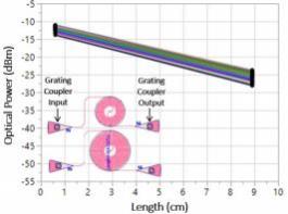
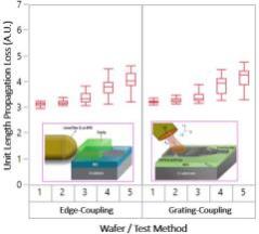
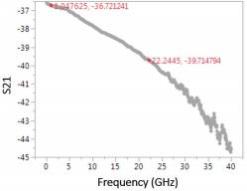
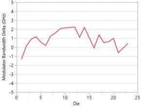
optical waveguides of different lengths using the cut-back method [3] outlined in Fig. 7, at length = 0 cm, each grating- coupler and edge-coupler loss can be accurately determined. When these coupling losses are subtracted and the normalized propagation losses determined by dividing with the total length of each optical waveguide, the measured results of optical waveguides with grating and edge-couplers correlate very well for all the 5 wafers presented in Fig. 8. This approach has also been validated for an optical modulator integrated circuit as shown in Fig 9, with good 3-dB bandwidth performance correlations for modulators fabricated with grating-couplers and edge-couplers.
IV. TEST STRUCTURE LAYOUT RULES AND STANDARDIZATION
Wafer-level characterization of photonics devices and circuits for wafer acceptance production tests involve DC, RF and optical measurements. To ensure devices can be successfully tested after the first pass design and wafer fabrication, layout design rules and orientation standardization ofDC test pads, RF test pads and optical grating-couplers around a device under test (DUT) must be established and communicated to circuit designers and device engineers. In this work, the minimum spacing between DC, RF test pads and keep-
out spacings around grating-couplers for fiber to scan above the grating-couplers are first determined and documented as a set of layout design rules.
The input and output optical grating-couplers are fixed on the east and west sides of the DUT while the DC and RF test pads are fixed in the north and south sides of the DUT respectively, as shown in Fig. 10. These rules and standardization ensure devices and circuits fabricated can be
successfully tested without probes and fibers colliding into each other. They also allow for motorized DC and RF positioners to be used with minimum probe-positioner setup changes to facilitate production wafer acceptance tests when characterizing different types of passive or active photonics devices and circuits.
V. WAFER-LEVEL PHOTONICS TEST AUTOMATION
A fully automatic 300mm engineering probe system with wafer loader, shown in Fig. 11(a), is used for the 24/7 photonics wafer acceptance production test. Fig. 11(b) reveals an optical calibration auxiliary chuck designed next to the main 300mm wafer chuck to support in-situ automatic single fiber and fiber array calibrations, edge-coupling fiber calibration as well as thermal optical wafer tests. Fig. 11(c) shows excellent fiber-to- grating-coupler repeatability of less than 0.1 dB for the fiber alignment positioning system when 100 alignment-cum-
measurements are made repeatably on each of the 3 optical waveguides across 3 dies. As photonics circuits require fiber to grating-coupler alignment, optical, DC, RF test signals, they are very complex, tedious and time consuming to test. Henceforth, an automatic test architecture, implemented with electrical and optical switches is required. For example, to test the optical modulator in Fig. 12, first step is to scan and align fibers to grating-couplers using a tunable laser source, polarization synthesizer and optical power meter. This is accomplished with the laser set at the wavelength of interest, tuned to an optimized polarization state. With this setup, the next step is to measure the extinction ratio (ratio of optical power levels for digital signals of “1” and “0”) by introducing DC bias tuning. The final step is to connect the output fiber from the optical power meter to the lightwave component analyzer (LCA) to measure the 3-dB bandwidth performance of the optical modulator. In this example, an optical switch that can be remotely controlled via GPIB (General Purpose Interface Bus), is used at the output fiber to toggle between the optical power meter and LCA so that a fully automatic test architecture can be achieved for a high precision and efficient photonics wafer test setup.
VI. CONCLUSION
Optical transceiver implemented with the silicon photonics technology is key in reducing the energy needed to operate data centers around the world. Accurate and efficient wafer-level photonics tests are crucial for KGD tests to enable 3DIC integration as well as to reduce product time-to-market. Optimizing the optical test setup, correlating results between wafer-level and final product tests, layout standardization as well as test architecture automation, are all critical in satisfying wafer acceptance production test requirements and they have been established and successfully demonstrated.
REFERENCES
[1] A. S. G. Andrae and T. Edler, “On Global Electricity Usage of
Communication Technology: Trends to 2030”, Challenges, Vol. 6, pp. 117-157, 2015.
[2] S. Nambiar, P. Sethi and S. K. Selvaraja, “Grating-Assisted Fiber to Chip
Coupling for SOI Photonic Circuits”, Applied Sciences, Vol. 8, pp. 1142,
2018.
[3] Yurii A. Vlasov and Sharee J. McNab, “Losses in single-mode silicon-on-
insulator strip waveguides and bends”, Optical Express, Vol. 12, Issue 8, pp. 1622-1631, 2014